
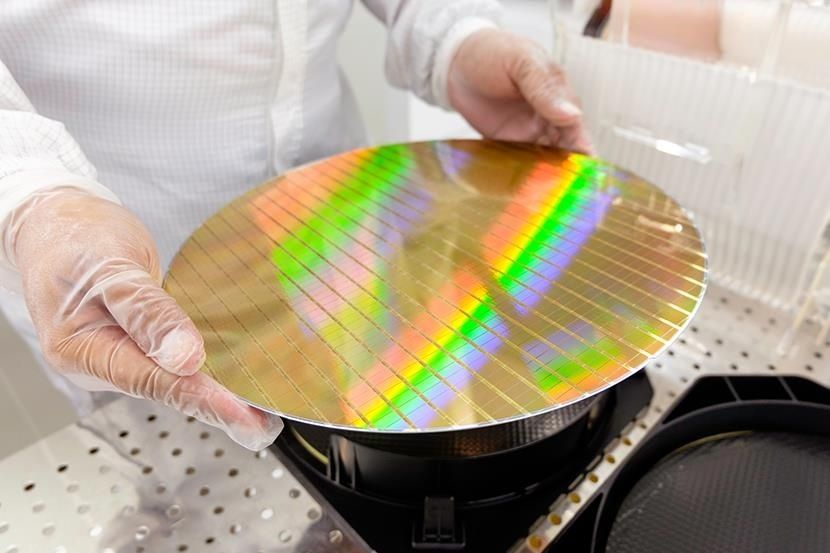
How Photolithography Prints Modern Microchips at the Nanoscale
The Sub-Nanometer Battleground in Modern Semiconductor Fabrication
Modern photolithography is no longer a simple projection process in which a reduced image of a mask is printed onto silicon. At advanced nodes, every exposed layer is the result of a tightly coupled optical, chemical, mechanical, and computational system. The practical objective is not merely to resolve a small line, but to place every edge within a narrow process window while controlling roughness, overlay, focus, dose, defects, and wafer-to-wafer variation. For engineers evaluating the future of chip manufacturing, the relevant question is how the entire exposure system behaves under these interacting constraints. That is why EUV lithography systems have become central to continued transistor scaling.
Classical deep ultraviolet lithography reached a difficult economic and physical threshold with 193 nm argon fluoride immersion systems. Increasing the numerical aperture by using water between the final lens and wafer improved resolution, but it did not remove the fundamental wavelength constraint. Further scaling required increasingly aggressive optical proximity correction, phase-shifting masks, spacer-defined patterning, and repeated exposure steps. Each additional patterning operation added alignment risk, process variation, defect opportunities, and cost. The result was a widening gap between nominal geometric capability and economically practical manufacturing.
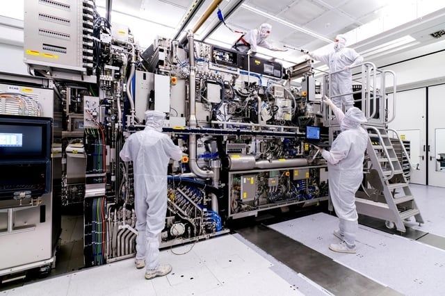
The transition to extreme ultraviolet light changes the roadmap by replacing the 193 nm wavelength with 13.5 nm radiation. That shift is large enough to reduce the dependence on multi-patterning for critical layers, but it introduces an entirely different machine architecture. EUV radiation must be generated from plasma, transported through vacuum, reflected by multilayer mirrors rather than transmitted through lenses, and registered by stages operating at high speed. This analysis examines the three engineering foundations of that transition: tin plasma source physics, reflective Bragg optics, and the anamorphic mechanics required for 0.55 numerical aperture High-NA tools.
Dissecting the Rayleigh Criterion for Advanced Process Nodes
The first-order resolution relationship in optical lithography is commonly expressed as CD = k1 x lambda / NA, where CD is the printed critical dimension, lambda is the exposure wavelength, NA is numerical aperture, and k1 represents the combined effect of illumination, mask design, resist behavior, and computational correction. The equation is not a complete process model, but it is an effective engineering framework. Lowering wavelength improves resolution linearly, as does increasing NA. Reducing k1 is possible through advanced imaging methods, although the available process margin shrinks rapidly as the value approaches its practical limit.
For 193 nm immersion lithography at an NA near 1.35, a nominal calculation with k1 equal to 0.30 gives a critical dimension of approximately 43 nm. In production, smaller pitches can be created through self-aligned double patterning and self-aligned quadruple patterning. SADP and SAQP divide a dense pattern into multiple process-defined spacings, but they do not provide a free resolution improvement. They require additional deposition, etch, spacer formation, cut-mask, and alignment operations. As k1 approaches the theoretical lower region near 0.25, the image becomes increasingly sensitive to focus, dose, mask three-dimensional effects, and resist nonlinearity.
| Architecture | Wavelength | Typical NA | Primary scaling advantage | Main penalty |
|---|---|---|---|---|
| ArF immersion | 193 nm | Approximately 1.35 | Mature tools and high throughput | Multi-patterning and overlay accumulation |
| Standard EUV | 13.5 nm | 0.33 | Fewer exposures for critical layers | Low source efficiency and stochastic resist behavior |
| High-NA EUV | 13.5 nm | 0.55 | Higher contrast and smaller printed dimensions | Smaller field, anamorphic optics, and higher mechanical complexity |
Using the same simplified equation, a 0.33 NA EUV system with k1 equal to 0.40 produces a nominal dimension of about 16.4 nm. A 0.55 NA High-NA system under the same k1 assumption produces approximately 9.8 nm. Actual technology-node labels do not directly equal printed single-pitch dimensions, because manufacturers use complex design rules, multiple pattern types, and process-specific definitions. Nevertheless, the comparison shows why the 13.5 nm wavelength is so valuable and why increasing NA remains important for sub-2nm logic.
The key trade-off is between optical simplicity and patterning complexity. A single EUV exposure can replace several DUV patterning steps, reducing cumulative overlay error and cycle time. However, EUV introduces expensive masks, low optical transmission, source maintenance, resist stochasticity, and demanding metrology. A process engineer must therefore compare not just nominal resolution, but the complete edge-placement error budget, defectivity, wafer-per-hour target, and number of critical layers. The best architecture is the one that minimizes total process variation at an acceptable cost, not necessarily the one with the smallest theoretical CD.
Engineering the 13.5 Nanometer EUV Source via Tin Droplet Plasma
EUV systems generally create 13.5 nm radiation through laser-produced plasma, or LPP. Tin is selected because highly ionized tin emits strong radiation near the desired wavelength through transitions in a complex ion population. The source must convert laser energy into useful in-band EUV radiation while limiting debris, maintaining repetition rate, and delivering stable dose to the scanner. This is an unusually demanding conversion chain because only a small fraction of the input laser power becomes usable radiation at the wafer.
The source begins with a droplet generator that dispenses molten tin at a repetition rate often described as approximately 50,000 droplets per second. Each droplet must have controlled diameter, velocity, spacing, and timing. The generator operates in a carefully managed thermal environment because tin must remain molten, yet the droplets must separate cleanly and arrive at the laser interaction point with micrometer-scale positional accuracy. A timing error at this stage directly becomes a dose fluctuation or source-utilization loss.
- A molten tin generator forms a regular stream of microscopic droplets.
- A low-energy prepulse strikes each selected droplet and reshapes it into a thin, pancake-like target.
- A high-power carbon dioxide laser pulse arrives after a controlled delay and rapidly ionizes the expanded tin.
- The resulting plasma emits broadband radiation, including the useful 13.5 nm band.
- A collector optic gathers and directs the EUV radiation into the scanner illumination system.
The prepulse is essential because a spherical droplet is not an efficient target for the main laser. Flattening increases the interaction area and improves coupling between the high-power CO2 pulse and the tin material. The second pulse creates the hot plasma required for EUV emission. Synchronization, laser stability, droplet placement, and plasma geometry must remain consistent over billions of exposure events. At the system level, source power is limited not only by laser energy, but also by debris control, collector lifetime, thermal management, and allowable dose variation.
Collector mirror degradation is one of the most difficult reliability problems. Tin ions, neutral atoms, and microscopic debris can contaminate the reflective surface, while the plasma and associated radiation generate substantial thermal load. Hydrogen buffer gas is used in portions of the source and collector environment to help remove contaminants and manage debris chemistry, but it also adds pumping and pressure-control requirements. Thermal loads can exceed 20 kilowatts in source regions, so cooling, shielding, and component replacement strategies become part of the scanner’s availability model. High source power is useful only when it translates into stable wafer throughput rather than frequent maintenance interruptions.
Reflective Bragg Optics and the Abolition of Refractive Lenses
At 13.5 nm, EUV radiation is absorbed by nearly all conventional optical materials, including glass and many gases. Air is therefore not a usable propagation medium, and standard refractive lenses cannot form an EUV projection system. The illumination path, mask environment, and projection optics must operate under high vacuum. This requirement affects the entire machine, including chamber design, vibration isolation, contamination control, pumping speed, thermal stability, and service procedures.
EUV projection optics instead use multilayer molybdenum-silicon mirrors. Each mirror contains repeated nanometer-scale layers selected so that reflections from the interfaces add constructively at the target wavelength and incidence angle. This distributed Bragg reflector principle produces useful reflectivity from a surface that would otherwise be inadequate at EUV wavelengths. The multilayer stack must maintain accurate thickness, interface quality, uniformity, and strain control across a large curved optic.
- Mo/Si layer thickness must remain tightly controlled to preserve the Bragg condition.
- Interface roughness must be extremely low, with specifications commonly discussed below 0.1 nm.
- Mirror figure errors directly affect focus, wavefront quality, and image placement.
- Contamination control is essential because a thin deposited film can reduce reflectivity and alter phase.
- Thermal expansion must be managed because nanometer-scale imaging is sensitive to minute shape changes.
Reflectivity is a cumulative system constraint. If each mirror reflects roughly 70 percent of the incident EUV power and the optical train contains more than ten reflective surfaces, the transmitted fraction declines rapidly. Ten idealized reflections at 70 percent efficiency leave only about 2.8 percent of the original power, before accounting for mask losses, spectral bandwidth, obscuration, and contamination. This explains why source power and collector efficiency are as important as the nominal resolution of the projection optics. Every optical surface must justify its presence through improved imaging performance or beam control.
The High-NA Paradigm and Anamorphic Lens Architecture
Standard EUV systems use a numerical aperture of 0.33. High-NA platforms increase this value to 0.55, improving image contrast and reducing the minimum printable dimension. The change is not a simple lens upgrade. Larger mirrors, tighter wavefront control, different illumination geometry, faster stages, and new mask handling systems are required. ASML describes its TWINSCAN EXE platform as the next EUV generation, with reported 8 nm resolution capability and a design aimed initially at advanced 2 nm logic and comparable-density memory applications.
High-NA optics also address mask three-dimensional effects through an anamorphic projection architecture. Instead of using the same magnification in both scan and slit directions, the system uses 8x magnification in one direction and 4x in the other. This allows the reticle size to remain compatible with established infrastructure while controlling shadowing and angular effects caused by the finite thickness and absorber geometry of EUV masks. The optical solution is elegant, but it creates a nonuniform imaging relationship that must be handled consistently by mask design, computational correction, inspection, and process control.
- Higher NA improves resolution but reduces depth of focus.
- Anamorphic magnification changes pattern scaling between the two field axes.
- Mask three-dimensional effects become more important at larger illumination angles.
- The exposure field is approximately halved, requiring more scan coverage for large dies.
- Reticle and wafer stages must accelerate and settle rapidly without increasing vibration or overlay error.
Halving the exposure field matters directly for large monolithic die architectures. A die that previously fit within one field may require a different layout strategy or multiple exposures with a stitching boundary. The wafer stage must support higher acceleration and precise synchronization with the reticle stage, while maintaining thermal and vibration stability. Faster movement cannot be treated as a pure throughput improvement because acceleration produces reaction forces, structural deformation, and control-loop demands.
Stitching introduces another overlay problem. If adjacent fields are joined across a critical region, the boundary must remain within a tight placement budget despite wafer distortion, stage error, reticle heating, and local process variation. This is especially important for large system-on-chip designs containing long interconnects, memory arrays, and analog interfaces that cross multiple functional regions. Before adopting a High-NA flow, manufacturers must evaluate die size, field utilization, stitching strategy, mask data preparation, inspection capability, and the total overlay budget rather than focusing only on the advertised resolution.
Edge Placement Error and Stochastic Yield Limits Below 2nm
Edge Placement Error, or EPE, is the displacement between the intended design edge and the edge actually formed on the wafer. It combines several contributors: optical proximity effects, lithography overlay, global reticle distortion, wafer distortion, focus and dose variation, resist processing, and etch transfer. At large dimensions, some errors can be averaged or absorbed by design margin. At sub-2nm technology generations, the same absolute error consumes a much larger fraction of the available pitch and can alter transistor performance, leakage, contact resistance, or timing.
Photon shot noise adds a statistical limit. EUV photons have higher energy than DUV photons, but the source-to-wafer conversion efficiency is low and optical losses are substantial. A finite number of photons reaches each local feature, so dose is not perfectly continuous. The resulting variation is amplified by photoelectron generation, secondary-electron scattering, resist chemistry, and development. Line-edge roughness can become a functional failure when roughness changes channel length or contact dimensions, while local underexposure or overexposure can create missing lines, breaks, or nano-bridges.
| EPE contributor | Physical origin | Engineering response |
|---|---|---|
| Optical proximity | Diffraction and neighboring feature interaction | Source optimization and OPC |
| Overlay | Layer-to-layer registration error | Stage control and alignment metrology |
| Reticle distortion | Heating, stress, and mask deformation | Thermal modeling and correction |
| Wafer distortion | Stress, topography, and processing history | Grid correction and wafer mapping |
| Stochastic variation | Photon and chemical randomness | Resist optimization and dose control |
Acid diffusion in chemically amplified resists creates a further compromise. More diffusion can improve sensitivity and development uniformity, but it blurs the latent image and increases uncertainty at feature edges. Less diffusion preserves resolution, yet may require higher dose or produce rougher, less stable patterns. Computational lithography must therefore model not only deterministic diffraction, but also mask three-dimensional behavior, resist response, etch bias, and stochastic variation. Advanced optical proximity correction and inverse lithography increasingly use physical models and machine-learning methods to search a huge mask-design space while preserving manufacturability.
In practice, yield improvement requires a closed loop connecting exposure data, metrology, defect inspection, and process control. A corrected mask is not sufficient if the wafer stage, resist track, plasma etch, or thermal environment introduces comparable errors. Below 2nm, the useful unit of optimization is the complete pattern-transfer chain. Computational lithography, high-resolution EPE metrology, source stabilization, and new resist platforms must be developed together.
Choosing a Sustainable Path Through Nanoscale Fabrication
Sub-2nm scaling is a combined economic and physical challenge. EUV scanners require extraordinary capital investment, specialized infrastructure, high-vacuum operation, precision optics, high-power lasers, contamination control, and extensive metrology. High-NA tools add anamorphic optics, smaller exposure fields, faster stages, and new integration requirements. These costs are justified only when the reduction in multi-patterning, cycle time, defects, and overlay accumulation improves the total manufacturing economics of the product.
The critical inflection point is the balance between adopting High-NA single exposure and extending 0.33 NA systems through additional patterning. Standard EUV remains valuable because it is established, broadly integrated, and capable of printing many advanced layers. High-NA becomes attractive when its higher resolution and reduced patterning count outweigh field-size penalties, tool cost, mask changes, and process-development risk. Future progress will depend on continuous gains in source power, collector lifetime, mirror contamination control, stage performance, EPE metrology, mask modeling, and photoresist chemistry. Moore’s law is therefore not being extended by one breakthrough component, but by the coordinated improvement of an entire precision manufacturing system.